
Recommended
More Related Content
What's hot
What's hot (20)
Viewers also liked
Viewers also liked (18)
Similar to Computer system architecture
Similar to Computer system architecture (20)
Recently uploaded
Recently uploaded (9)
Computer system architecture
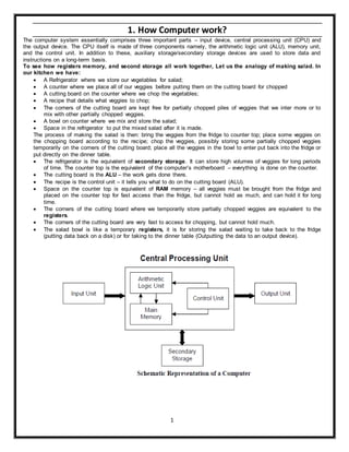
- 1. 1 1. How Computer work? The computer system essentially comprises three important parts – input device, central processing unit (CPU) and the output device. The CPU itself is made of three components namely, the arithmetic logic unit (ALU), memory unit, and the control unit. In addition to these, auxiliary storage/secondary storage devices are used to store data and instructions on a long-term basis. To see how registers memory, and second storage all work together, Let us the analogy of making salad. In our kitchen we have: A Refrigerator where we store our vegetables for salad; A counter where we place all of our veggies before putting them on the cutting board for chopped A cutting board on the counter where we chop the vegetables; A recipe that details what veggies to chop; The corners of the cutting board are kept free for partially chopped piles of veggies that we inter more or to mix with other partially chopped veggies. A bowl on counter where we mix and store the salad; Space in the refrigerator to put the mixed salad after it is made. The process of making the salad is then: bring the veggies from the fridge to counter top; place some veggies on the chopping board according to the recipe; chop the veggies, possibly storing some partially chopped veggies temporarily on the corners of the cutting board; place all the veggies in the bowl to enter put back into the fridge or put directly on the dinner table. The refrigerator is the equivalent of secondary storage. It can store high volumes of veggies for long periods of time. The counter top is the equivalent of the computer’s motherboard – everything is done on the counter. The cutting board is the ALU – the work gets done there. The recipe is the control unit – it tells you what to do on the cutting board (ALU). Space on the counter top is equivalent of RAM memory – all veggies must be brought from the fridge and placed on the counter top for fast access than the fridge, but cannot hold as much, and can hold it for long time. The corners of the cutting board where we temporarily store partially chopped veggies are equivalent to the registers. The corners of the cutting board are very fast to access for chopping, but cannot hold much. The salad bowl is like a temporary registers, it is for storing the salad waiting to take back to the fridge (putting data back on a disk) or for taking to the dinner table (Outputting the data to an output device).
- 2. 2 2. Logic • Formal logic is a branch of mathematics that deals with true and false values instead of numbers. • In the mid-19th century, GEORGE BOOL developed many Logic ideas. • Boolean logic deals with equations where the operators are “AND” or “OR” instead of “add” and “multiply”. Electric Logic • Logical values can easily be expressed by an electrical circuit. • “True” or “1” can be defined as voltage on a wire while “False” or “0” can be defined as no voltage. We will use positive logic. • Analog values can be anything while digital only has discrete values, 0 or 1 • Electrical devices called “gates” can implement the logical Logic Gates 1. OR gate The OR gate is an electronic circuit that gives a true output (1) if one or more of its inputs are true. A plus (+) is used to show the OR operation 2. AND gate The AND gate is an electronic circuit that gives a true output (1) only if all its inputs are true. A dot (·) is used to show the AND operation i.e. A·B. Note that the dot is sometimes omitted i.e. AB . 3. NAND gate This is a NOT-AND gate which is equal to an AND gate followed by a NOT gate. • The outputs of all NAND gates are true if any of the inputs are false. • The symbol is an AND gate with a small circle on the output. The small circle represents inversion 4. NOR gate This is a NOT-OR gate which is equal to an OR gate followed by a NOT gate. • The outputs of all NOR gates are false if any of the inputs are true. • The symbol is an OR gate with a small circle on the output. The small circle represents inversion. 5. EX-OR gate The 'Exclusive-OR' gate is a circuit which will give a true output if either, but not both, of its two inputs are true. • An encircled plus sign ( ) is used to show the EOR operation. 6. EX-NOR gate The 'Exclusive-NOR' gate circuit does the opposite to the EOR gate. • It will give a false output if either, but not both, of its two inputs are true. • The symbol is an EXOR gate with a small circle on the output. • The small circle represents inversion. Three Input AND Gate • Here is an example of a three input AND gate. • Notice that the truth table for the three input gate is similar to the truth table for the two input gate. • It works on the same principle, this time all three inputs need to be true (1) to get a true output.
- 3. 3 3. Logic circuit An electronic circuit used in computers to perform a logical operation on its two or more input signals. Types of logic circuit:- 1. Sequential circuit 2. Combinational circuit Sequential circuit:- In digital circuit theory, sequential logic is a type of logic circuit whose output depends not only on the present value of its input signals but on the sequence of past inputs, the input history. Sequential logic is used to construct finite state machines, a basic building block in all digital circuitry, as well as memory circuits and other devices. e.g. Flip flop or latch Combinational circuit:- It is a type of digital logic which is implemented by Boolean circuits, where the output is a pure function of the present input only. They do not have any memory elements. e.g. Adder, decoder, encoder, multiplexer. Combinational logic circuits: Sequential logic circuits: Outputs depend only on its current inputs. Outputs depend not only on the current inputs but also on the past sequences of inputs. A combinational circuit may contain an arbitrary number of logic gates and inverters but no feedback loops. A feedback loop is a connection from the output of one gate to propagate back into the input of that same gate Sequential logic circuits contain combinational logic in addition to memory elements formed with feedback loops. The function of a combinational circuit represented by a logic diagram is formally described using logic expressions and truth tables. The behavior of sequential circuits is formally described with state transition tables and diagrams. Circuit Memory INPUT OUTPUT Combinational Circuit I1 I2 I3 n O1 O2 O3 m
- 4. 4 4. Flip Flop or Latch The memory elements in a sequential circuit are called flip-flops. A flip-flop circuit has two outputs, one for the normal value and one for the complement value of the stored bit. Binary information can enter a flip-flop in a variety of ways and gives rise to different types of flip-flops. Latch (level triggered) o R-S Latch o D Latch Flip Flop(edge triggered) o J-K Flip-Flop o T Flip Flop o Master-Slave Flip-Flop R-S Latch R-S latch has two inputs, labeled RESET and SET. If the SET input is HIGH, the Q output goes HIGH. If the RESET input is HIGH, the Q output goes LOW. Note that in an SR latch, the SET and RESET inputs shouldn't both be HIGH when the clock is triggered. This is considered an invalid input condition, and the resulting output isn't predictable if this condition occurs. Here's a basic circuit that involves just two NAND gates. There are two inputs to this circuit, R and S. Can you generate a truth table for this circuit? How to work R-S latch If R = 0, then Q = 1. We know that if either input to a NAND gate is 0, the output is 1. Now try to take advantage of the knowledge that Q = 1. If Q = 1 AND S = 0, then Q’ = 1. It doesn't matter what Q is, as long as S = 0, Q will be 1. Finally, we have the case where R = 1 and S = 1. If R = 1, Q will be either 0 or 1. If we assume 0 then S=1 and Q’ will be 1. If S = 1, Q’ will be either 0 or 1. If we assume 0 then R=1 and Q will be 1. The state of the flip-flop is indeterminate( not able to be stated) D Flip-Flop It has just one input in addition to the CLOCK input. This input is called the DATA input. The Q output is matched to the DATA input. Thus, if the DATA input is HIGH, the Q output goes HIGH, and if the DATA input is LOW, the Q output goes LOW. Most D-type flip-flops also include S and R inputs that let you set or reset the flip-flop. Note that the S and R inputs in a D flip-flop ignore the CLOCK input. Thus, if you apply a HIGH to either S or R, the flip-flop will be set or reset immediately, without waiting for a clock pulse. J-K Flip-Flop JK means Jack Kilby, a Texas instrument engineer who invented IC. JK flip-flop is a refinement of RS flip- flop. A JK flip-flop has two inputs, labeled J and K. The J input corresponds to the SET input in an SR flip-flop, and the K input corresponds to the RESET input. The difference between a JK flip-flop and an SR flip-flop is that in a JK flip-flop, both inputs can be HIGH. When both the J and K inputs are HIGH, the Q output is toggled, which means that the output alternates between HIGH and LOW. When J=K=0 When both J and K are 0, the clock pulse has no effect on the output and the output of the flip-flop is the same as its previous value. This is because when both the J and K are 0, the output of their respective AND gate becomes 0. When J=0, K=1
- 5. 5 When J=0, the output of the AND gate corresponding to J becomes 0 (i.e.) S=0 and R=1. Therefore Q’ becomes 0. This condition will reset the flip-flop. This represents the RESET state of Flip-flop. When J=1, K=0 In this case, the AND gate corresponding to K becomes 0(i.e.) S=1 and R=0. Therefore Q becomes 0. This condition will set the Flip-flop. This represents the SET state of Flip-flop. When J=K=1 Consider the condition of CP=1 and J=K=1. This will cause the output to complement again and again. This complement operation continues until the Clock pulse goes back to 0. Since this condition is undesirable, we have to find a way to eliminate this condition. This undesirable behavior can be eliminated by Edge triggering of JK flip-flop or by using master slave JK Flip-flops. T Flip-Flop T flip-flops are similar to JK flip-flops. T flip-flops are single input version of JK flip-flops. This modified form of JK flip-flop is obtained by connecting both inputs J and K together. This flip-flop has only one input along with Clock pulse. These flip-flops are called T flip-flops because of their ability to complement its state (i.e.) Toggle. So they are called as Toggle flip-flop. When T=1 and CP=1, the flip-flop complements its output, regardless of the present state of the Flip-flop. In this case the next state is the complement of the present state. When T=0, there is no change in the state of the flip-flop (i.e.) the next state is same as the present state of the flip-flop. From the characteristic table and characteristic equation it is quite evident that when T=0, the next sate is same as the present state. Master Flip-Flop The circuit of Master-Slave Flip Flop is basically two flip-flops connected serially. The first flip-flop is called the Master and the second is termed Slave. In a Master-Slave Flip Flop inputs are fed at the +ve edge and output is available at the -ve edge. Let Q (t) and Q (t+1) represent the present state and next state of the flip flop, here is the truth table and circuit diagram of a Master-Slave Flip Flop: Clock is connected directly to Master and inverted to Slave. When clock is high – Master is functional and when clock is low – Slave is functional. Thus, what a master flip-flop does when the clock goes high, the slave flip-flop copies when the clock goes low. For example, when J=1, K=1, let Q (t) = 0 and Q’ (t) = 1. When clock is high then Q (t+1) = 1, Q’ (t+1) = 0. When clock is low then Q (t+1) = 1, Q’ (t+1) = 0. Thus, even when J=1, K=1, the outputs are complement to each other.
- 6. 6 What's a Clock? A clock is a device that alternates between 0 and 1, repeatedly. We can define key features of this plot. The most important is the amount of time it takes before the signal repeats. This time is called the period, which we call T. In this period, there is a single cycle. The period is related to the frequency, f. In fact, they are inversely related f = 1/T. The frequency means how many times the waveform repeats per second. The unit of measurement for frequency is Hz (pronounced Hertz), and is the same as s-1 (inverse seconds). The higher the frequency, the shorter the period of one cycle. When you hear a clock is 1 GHz, this means there is 109 cycles per second (G = giga = 109). Consequently, the period is 10-9seconds, which is a nanosecond. The behavior of a clock can be easily described using a timing diagram. A timing diagram has time on the horizontal axis (x-axis) and the voltage on the vertical axis (y-axis). For simplicity, we use 0 and 1, instead of voltages. Triggering of flip-flop Level-triggering is the transfer of data from input to output of a flip flop anytime the clock pulse is proper voltage level. Edge-triggering is the transfer of data from input to output of flip-flop on rising edge (L-to-H) or falling edge (H- to-L) of the clock pulse. Edge triggering may be either positive-edge (l-to-H or negative-edge (H-to-L).
- 7. 7 5. Combinational logic circuit Encoder An encoder is a combinational logic circuit that essentially performs a “reverse” of decoder functions. An encoder accepts an active level on one of its inputs, representing digit, such as a decimal or octal digits, and converts it to a coded output such as BCD or binary. Encoders can also be devised to encode various symbols and alphabetic characters. The process of converting from familiar symbols or numbers to a coded format is called encoding. Most decoders accept an input code and produce a HIGH or a LOW at one and only one output line. a decoder identifies, recognizes, or detects a particular code. The opposite of this decoding process is called encoding and is performed by a logic circuit called an encoder. An encoder has a number of input lines, only one of which input is activated at a given time and produces an N-bit output code depending on which input is activated. An encoder has 2n inputs n outputs Priority Encoders A priority encoder is an circuit that includes the priority function. If more than one input is active, the higher-order input has priority over the lower-order input. o The higher value is encoded on the output A valid indicator, d, is included to indicate whether or not the output is valid. o Output is invalid when no inputs are active d = 0 o Output is valid when at least one input is active d = 1
- 8. 8 Decoder A binary code of n bits is capable of representing up to 2^n distinct elements of coded information. A decoder is a combinational circuit that converts binary information from n input lines to a maximum of 2^n unique output lines. If the n-bit coded information has unused combinations, the decoder may have fewer than 2^n outputs The decoder is a commonly used type of integrated circuit. 3-8 decoder This decoder generates all of the min-terms of the three input variables. Exactly one of the output lines will be 1 for each combination of the values of the input variables. 4*16 decoder constructed with two 3*8 decoder Decoders with enable inputs can be connected together to form a larger Decoder circuit. This shows two 3-to-8-line decoders with enable inputs connected to form a 4-to-16-line decoder. When w = 0, the top decoder is enabled and the other is disabled. The bottom decoder outputs are all 0’s, and the top eight outputs generate minterms 0000 to 0111. When w = 1, the enable conditions are reversed: The bottom decoder outputs generate minterms 1000 to 1111, while the outputs of the top decoder are all 0’s. Multiplexers A multiplexer has o 2n data inputs o n control inputs o 1 output A multiplexer routes (or connects) the selected data input to the output. The value of the control inputs determines the data input that is selected.
- 9. 9 Registers A flip-flop stores one bit of information. When a set of n flip-flops is used to store n bits of information, such as an n-bit number, we refer to these flip-flops as a register. A common clock is used for each flip-flop in a register; Shift Register A given number is multiplied by 2 if its bits are shifted one bit position to the left and a 0 is inserted as the new least-significant bit. Similarly, the number is divided by 2 if the bits are shifted one bit-position to the right. A register that provides the ability to shift its contents is called a shift register. A four-bit shift registers A four-bit shift register that is used to shift its contents one bit position to the right, the data bits are loaded into the shift register in a serial fashion using the input. The contents of each flip-flop are transferred to the next flip-flop at each positive edge of the clock. To implement a shift register, it is necessary to use either edge-triggered or master-slave Flip-flops. The level-sensitive gated latches are not suitable, because a change in the value of in would propagate through more than one latch during the time when the clock is equal to 1.
- 10. 10 Parallel-Access Shift Register In computer systems it is often necessary to transfer n-bit data items. This may be done by transmitting all bits at once using n separate wires, in which case we say that the transfer is performed in parallel. But it is also possible to transfer all bits using a single wire, by performing the transfer one bit at a time, in n consecutive clock cycles. We refer to this scheme as serial transfer. To transfer an n-bit data item serially, we can use a shift register that can be loaded with all n bits in parallel (in one clock cycle). Then during the next n clock cycles, the contents of the register can be shifted out for serial transfer. The reverse operation is also needed. If bits are received serially, then after n clock cycles the contents of the register can be accessed in parallel as an n-bit item. A four-bit shift register that allows the parallel access.Instead of using the normal shift register connection, the D input of each flip-flop is connected to two different sources.One source is the preceding flip-flop, which is needed for the shift register operation. The other source is the external input that corresponds to the bit that is to be loaded into the flip -flop as a part of the parallel-load operation. The control signal Shift/Load is used to select the mode of operation. If Shift/Load = 0, then the circuit operates as a shift register. If Shift/Load = 1, then the parallel input data are loaded into the register. In both cases the action takes place on the positive edge of the clock.
- 11. 11
- 12. 12 6. Computer buses It is a set of parallel lines used to connect two or more devices of a digital computer. It is the most important component of computer architecture. A computer has more the one bus interconnection. All the components of computer are connected with a set of parallel lines. All these lines are used to transfer data in the form of bits from one component to another component. These lines are called BUS. There are two types of buses: o System bus o Expansion Bus System Bus System bus is used to connect main components of the computer (main memory, CPU, I/O devices). Generally there are 70-100 parallel lines in system bus. Every parallel line is used to transfer a single bit at a time. It is divided into three main categories. o Control Bus o Address bus o Data Bus Control Bus: These lines are used to transfer control signal from one component to other. It specifies the type of operation that is to be performed. It also transmits the control signals like ACKS (acknowledgement signal). When a CPU command to the memory for writing data, then the memory send an acknowledgement signal to the CPU after successful writing of data. Control bus is bi-directional. Write some commands related to bus interconnection. Command Purpose MEMORY WRITE Write data to a given location in main memory. MEMORY READ Read data from a given output device. I/O WRITE Write data to a given output device. I/O READ Read data from a given input device. BUS REQUEST Request for a control on the bus for transmitting data. BUS GRANT Indicate the grant of the bus to a device. TRANSFER ASK This command is used to request for data transfer Address Bus It is a part of system bus. It is used to carry address signals to read and write data in the memory. Address bus is uni-directional. An address is a unique ID of each component connected to the system bus. It is called address of the component. Data Bus Data bus is used to transfer the data from one component to another. There are 32 or 64 parallel lines of data bus. The amount of data that a bus can transmit is called bus-width. A 64-bit data bus can transmits 64 bits (8 bytes) at a time.
- 13. 13 Maximum RAM for 32-bit: 4GB Maximum RAM for 64-bit: 16EB (16 Billion GB) Width of data bus has direct impact on the performance of the computer. Data bus is bi-directional. Expansion Bus The major components are connected to the system bus and the remaining components are connected to expansion bus and the expansion bus is connected to the system bus. If all the components are attached with system bus then it will slow the computer. All the components will have to wait longer to get access to the bus. We use the expansion bus to solve this problem. Bus and data Transfer A bus structure consist a set of common lines each for each register, through which binary information can transfer one at time. Control signal determine that which register is connected with a bus line at time to transfer the information. Here we will see two ways to construct the bus : o By using multiplexers. o By three state buffer. By using multiplexers, The multiplexer select the one register who‘s information is transfer to another one destination register. In a bus system, multiplex K register of n bits each to produce an n lines common bus . The number of multiplexers needed to construct the bus is equal to n. Size of each MUX is must be k-1 multiplexer hence multiplexer have n data lines. (Example: For common bus system using multiplexer for 16 register each of 32 bit data transformation. solution: In this system we require 32(number of bits) multiplexer each having size of 16-1 multiplexer(number of register) and number of selection inputs are 4) The construction of bus system for four bit, four register is given below: As we know that for n bit we require n multiplexer, for k register transfer we require k-1 size of multiplexer. Here we have n=4 and k=4 hence here we use four multiplexer each having 4-1 size. Here each register have 4 positive triggered flip- flop set. Because each MUX is 4-1 each multiplexer have 2 selection inputs in the bus. We denote it by S0 and S1. This selection input select the one line output from 0 to 3 available in the each multiplexer, and applied to the output that form a bus system. To avoid the complicated figure we just write output and input at the connection. For example output A1 of register A is connected with the input line 0 of MUX (1) because that input is labeled as A1. The two selection lines S0 and S1 are connected to the selection inputs of all four multiplexers. The selection lines choose the four bits of one register and transfer them into the four-line common bus. When S1S0 =00, the 0 data inputs of all four multiplexers are selected and applied to the outputs that form the bus. This causes the bus lines to receive the content of register A since the outputs of this register are connected to the 0 data inputs of the multiplexers. Similarly, register B is selected if S1S0= 0 1, and so on.
- 14. 14 Memory Transfer The transfer of information from a bus into one of many destination registers can be accomplished by connecting the bus lines to the inputs of all destination registers and activating the load control of the particular destination register selected. The transfer of information from a memory word to the outside environment is called a read operation. The content of register C is placed on the bus, and the contents of the bus is loaded into the register R1 by activating its load control input. The symbolic statement for a bus transfer may mention the bus or its presence may be implied in the statement. BUS C When the bus is included in the statement, the register transfer is symbolized as follows. R1 BUS The transfer of new information to be stored into the memory is called a write operation. A memory word will be symbolized by the letter M. The particular memory word among the many available is selected by the memory address during the transfer. It is necessary to specify the address of M when writing memory transfer operations. This will be done by enclosing the address in square brackets following the letter M. The address register, symbolized by AR. The data are transferred to another register, called the data register, symbolized by DR. The read operation can be stated as follows: Read: DR M [AR] Memory, write this causes a transfer of information into DR from the memory word M selected by the address in AR. The write operation transfers the content of a data register to a memory word M selected by the address. Assume that the input data are in register R1 and the address is in AR. The write operation can be stated symbolically as follows: Write: M [AR] R1 By three state buffer A bus System can also be implemented by using a three-state buffer and a decoder instead of multiplexers. A three state gate exhibits three states, namely, state with output 1, state with output 0 or a high impedance at the output. High impedance state means that the output gets disconnected and will have no logical significance. In a three state buffer gate, there are two inputs. One is a normal input and the other a Control Input(CI). The output from the buffer gate would be same as the input given, o If CI=1 and input=0 the output = 0. o If CI=1 and input=1 the output = 1. o If CI=0 and input=0 the output = high impedance (Z). o If CI=0 and input=1 the output = High impedance (Z). Bus System with Three State Buffer The inputs to the four buffer gates are the 0th bit of the four registers A, B, C and D, Namely A0, B0, C0, D0. One way to ensure that no more than one control input is active at any given time is to use a decoder. When the enable input of the decoder is 0, all of its four outputs are 0, and the bus line is in a high-impedance state because all four buffers are disabled. When the enable input is active, one of the three-state buffers will be active, depending on the binary value in the select inputs of the decoder. We will require four buffers for each register. The 0th output of the decoder will be connected to all the four buffers of register A. The 1th output of the decoder will be connected to all the four buffers of register B. The 2th output of the decoder will be connected to all the four buffers of register C. The 3th output of the decoder will be connected to all the four buffers of register D. Control Input(CI) Input Output 0 0 Z 0 1 Z 1 0 0 1 1 1
- 15. 15 7. Motherboard The motherboard (sometimes called the main board) is the main circuit board inside a personal computer. Other vital system components like the central processing unit (CPU) and random access memory (RAM) modules are connected directly to the motherboard via slots or sockets designed specifically for those components. The motherboard will also provide a number of expansion slots designed to accommodate add-on cards such as video graphics adapter (VGA) cards and network interface cards (NICs). Various other connectors and ports are built in to the motherboard to enable the connection of both internal secondary storage devices such as Hard disk drives and optical drives, and peripheral (external) devices such as a mouse, keyboard and printer There are also sockets to allow the motherboard to be connected to a suitable power supply unit (PSU). The motherboard is effectively a backplane that connects together all of the devices that make up a. It also supplies power to many of those devices. The microchips soldered to the motherboard provide various system control functions to enable the CPU to concentrate on its main role, which is the execution of programs. This collection of microcontrollers is sometimes referred to as the motherboard's chipset, although a narrower definition of the term refers to two main chips (the so-called north bridge and south bridge) that provide the communications interface between the core components and the rest of the system. The connections linking the various components, ports and sockets on the motherboard are used to carry data and control signals between them, and are often referred to as buses. Because of the sheer number of connections required on a modern motherboard, most of the connections consist of very narrow metal tracks called traces. Many of the signals being sent backwards and forwards between the main system components such as the CPU and main memory have very high frequencies. The chipset The chipset is a collection of microcontroller chips that provides a high-speed communications interface between the main system components and carries out many of the low-level hardware control functions, allowing the processor to spend most of its time executing program instructions. The chipset is carefully designed to work with a particular processor or range of processors in order to maximize performance while at the same time keeping down the cost of the system. The two most important chips on the motherboard provide the system's core logic, and have come to be known as the north bridge (also referred to as the memory controller hub) and the south bridge (otherwise known as the I/O Controller Hub), which take their respective names from their relative positions on the motherboard. Between them, these two chips encompass many of the most important communications and control functions provided by the motherboard (the term "chipset" is often taken to refer specifically to just these components). The generic block diagram below shows the main features and layout of a typical modern motherboard. North Bridge The North Bridge (also known as the MEMORY CONTROLLER HUB) is connected directly to the processor via the front-side bus, to system memory via the memory bus, and to the south bridge via an internal bus. It is also typically connected to a high speed graphics card slot via either an accelerated graphics port (AGP) bus or a PCI Express (PCI-E) bus, depending on the type of slot provided. The communication handled via the north bridge (i.e. between the CPU, memory and video card) requires the use of high-speed buses. The CPU gains fast access to memory via a memory controller built in to the north bridge. The speed with which the processor can retrieve data from memory is one of the most important factors in determining how fast in can
- 16. 16 execute programs, and the sheer volume of data required for modern graphic-intensive applications make the availability of a high-speed dedicated AGP or PCI-E bus essential. South bridge Those parts of the system requiring (relatively) low-speed communications are connected to the Northbridge via the Southbridge (also known as the I/O CONTROLLER HUB). The buses connecting the Southbridge with the motherboard's expansion slots and integrated peripherals such as an on-board graphics adapter are typically PCI buses. A low pin count (LPC) bus connects the Southbridge to BIOS, and to the Super I/O chip which provides a control interface for low-bandwidth devices such as the keyboard and mouse, as well as devices that connect via a serial or parallel port. Higher-speed interfaces such as IDE, SATA and USB have their own buses. Front-side Bus FSB is also known as the Processor Bus, Memory Bus, or System Bus and connects the CPU (chipset) with the main memory and L2 cache. The FSB can range from speeds of 66 MHz, 133 MHz, 100 MHz, 266 MHz, 400 MHz, and up. PCI Bus (component bus) Short for Peripheral Component Interconnect, PCI was introduced by Intel in1992. The PCI bus came in both 32- bit (133MBps) and 64-bit versions and was used to attach hardware to a computer. Expansion Slot Alternatively referred to as a bus slot or expansion port, an expansion slot is connection or port located inside a computer on the motherboard or riser board that allows a computer hardware expansion card to be connected. For example, if you wanted to install a new video card in the computer, you'd purchase a video expansion card and install that card into the compatible expansion slot. AGP Short for Accelerated Graphics Port, AGP is an advanced port designed for Video cards and 3D accelerators. Designed by Intel and introduced in August of 1997, AGP introduces a dedicated point-to-point channel that allows the graphics controller direct access to the system memory. Below is an illustration of what the AGP slot may look like on your motherboard. AMR Released September 8, 1998, AMR is short for Audio/Modem Riser and allows OEMs to make one card that has the functionality of either Modem or Audio or both Audio and Modem on one card. This specification allows for the motherboard to be manufactured at a lower cost and free up industry standard expansion slots in the system for other additional plug-in peripherals. CNR Short for Communication and Network Riser, CNR is a specification that supports Audio, Modem, USB, and LAN interfaces of core logic chipsets. This technology and the CNR slot was first introduced by Intel February 7, 2000 and was mainly developed by leading hardware and software developers who helped release the AMR (Audio Modem Riser) slot. In the picture below is an example of a CNR slot, which is labeled as "CNR_SLOT" on this motherboard. Traces Small lines of copper or aluminum that connect each of the IC, capacitors, resistors, and other components on a circuit board together. The picture is an example of what circuit traces look like on a motherboard.
- 17. 17 8. ALU Short for Arithmetic Logic Unit, the ALU is a complex digital circuit; one of many components within a computer's central processing unit. It performs both bitwise and mathematical operations on binary numbers and is the last component to perform calculations in the processor. The ALU uses to operands and code that tells it which operations to perform for input data. After the information has been processed by the ALU, it is sent to the computer's memory. Multiple Arithmetic Logic Units can be found in CPUs, GPUs and FPUs. In some computer processors, the ALU is divided into an AU and LU. The AU performs the arithmetic operations, and the LU performs the logical operations. Arithmetic operations: Add: A and B are summed and the sum appears at Y and carry-out.(Half-Adder) Add with carry: A, B and carry-in are summed and the sum appears at Y and carry-out.(Full- Adder) Subtract: B is subtracted from A (or vice-versa) and the difference appears at Y and carry-out. For this function, carry-out is effectively a "borrow" indicator. This operation may also be used to compare the magnitudes of A and B; in such cases the Y output may be ignored by the processor, which is only interested in the status bits (particularly zero and negative) that result from the operation.(Half-subtractor) Subtract with borrow: B is subtracted from A (or vice-versa) with borrow (carry-in) and the difference appears at Y and carry-out (borrow out).(Full- Subtractor) Two's complement (negate): A (or B) is subtracted from zero and the difference appears at Y. Increment: A (or B) is increased by one and the resulting value appears at Y. Decrement: A (or B) is decreased by one and the resulting value appears at Y. Pass through: all bits of A (or B) appear unmodified at Y. This operation is typically used to determine the parity of the operand or whether it is zero or negative. Binary Addition Circuits Logic gates are used to accomplish the arithmetic operation of binary addition in digital circuits. A two input logic gate is required to accomplish the addition of two binary numbers. The exclusive-OR gate is used to achieve binary addition which is slightly different from basic OR gate.
- 18. 18 Half-Adder A logic circuit block used for adding two one bit numbers or simply two bits is called as a half adder circuit. This circuit has two inputs which accept the two bits and two outputs, with one producing sum output and other produce carry output. Binary addition is commonly performed by Ex-OR gate, but for the first three rules, it performs the binary addition and when the two inputs are logic 1, it does not develop any carry. To accomplish the binary addition with Ex-OR gate, there is need of additional circuitry to perform the carry operation. Hence, a half adder is formed by connecting AND gate to the input terminals of the Ex-OR gate so as to produce the carry. Half adder has limited number of applications, and practically not used in the application especially multi-digit addition. Full Adder A binary full adder is a multiple output combinational logic network that performs the arithmetic sum of three input bits. As we have seen that the half adder cannot respond to the three inputs and hence the full adder is used to add three digits at a time. It consists of three inputs, in which two are input variables represent the two significant bits to be added, labeled as A and B, where as the third input terminal is the carry from the previous lower significant position and labeled as Cin. The two outputs are a sum and a carry outputs which are labeled as ∑ and Cout respectively. Full adder can be formed by combining two half adders and an OR gate as shown in above where output and carry- in of the first adder becomes the input to the second half adder that produce the total sum output. The total carry out is produced by ORing the two half adder carry outs as shown in figure. The full adder block diagram and truth table is shown below. Parallel Binary Adders For performing the addition of binary numbers with more than one bit, more than one full adder is required depends on the number bits. Thus, a parallel adder is used for adding all bits of the two numbers simultaneously. By connecting a number of full adders in parallel, n-bit parallel adder is constructed. From the below figure, it is to be noted that there is no carry at the least significant position, hence we can use either a half adder or made the carry input of full adder to zero at this position.
- 19. 19 Binary Subtraction Circuits Subtraction is a mathematical operation in which one integer number is deducted from another to obtain the equivalent quantity. The number from which other number is to be deducted is called as minuend and the number subtracted from the minuend is called subtrahend. Similar to the binary addition, binary subtraction is also has four possible alternative operations. The above figure shows the four possible rules or elementary operations of the binary subtractions. In all the operations, each subtrahend bit is deducted from the minuend bit. But in the second rule, minuend bit is smaller than the subtrahend bit, hence 1 is borrowed to perform the subtraction. Similar to the adder circuits, subtraction circuits are also classified as half subtractors, full subtractors and parallel subtractors. Half Subtractors A half subtractor is a multiple output combinational logic network that does the subtraction of two bits of binary data. It has input variables and two output variables. Two inputs are corresponding to two input bits and two output variables correspond to the difference bit and borrow bit. The binary subtraction is also performed by the Ex-OR gate with additional circuitry to perform the borrow operation. Thus, a half subtractor is designed by an Ex-OR gate including AND gate with A input complemented before fed to the gate. The block model, truth table and logic diagram of a half subtractor shown in above figure. This circuit is similar to the half adder with only difference in input A i.e., minuend which is complemented before applied at the AND gate to implement the borrow output. In case of multi-digit subtraction, subtraction between the two digits must be performed along with borrow of the previous digit subtraction, and hence a subtractor needs to have three inputs. Therefore, a half subtractor has limited applications and strictly it is not used in practice.
- 20. 20 Full Subtractor A combinational logic circuit performs a subtraction between the two binary bits by considering borrow of the lower significant stage is called as the full subtractor. In this, subtraction of the two digits is performed by taking into consideration whether a 1 has already borrowed by the previous adjacent lower minuend bit or not. It has three input terminals in which two terminals corresponds to the two bits to be subtracted (minuend A and subtrahend B), and a borrow bit Bi corresponds to the borrow operation. There are two outputs, one corresponds to the difference D output and other borrow output Bo as shown in figure along with truth table. By deriving the Boolean expression for the full subtractor from above truth table, we get the expression that tells that a full subtractor can be implemented with half subtractors with OR gate as shown in figure below. By comparing the adder and subtractor circuits or truth tables, one can observe that the output D in the full subtractor is exactly same as the output S of the full adder. And the only difference is that input variable A is complemented in the full subtractor. Therefore, it is possible to convert the full adder circuit into full subtractor by simply complementing the input A before it is applied to the gates to produce the final borrow bit output Bo. Parallel Binary Subtractors To perform the subtraction of binary numbers with more than one bit is performed through the parallel subtractors. This parallel subtractor can be designed in several ways, including combination of half and full subtractors, all full subtractors, all full adders with subtrahend complement input, etc. The below figure shows a 4 bit parallel binary subtractor formed by connecting one half subtractor and three full subtractors. In this subtractor, 4 bit minuend A3A2A1A0 is subtracted by 4 bit subtrahend B3B2B1B0 and gives the difference output D3D2D1D0. The borrow output of each subtractor is connected as the borrow input to the next preceding subtractor. Parallel Adder / Subtractor The operations of both addition and subtraction can be performed by a one common binary adder. Such binary circuit can be designed by adding an Ex-OR gate with each full adder as shown in below figure. The figure below shows the 4 bit parallel binary adder/subtractor which has two 4 bit inputs as A3A2A1A0 and B3B2B1B0 The mode input control line M is connected with carry input of the least significant bit of the full adder. This control line decides the type of operation, whether addition or subtraction. When M= 1, the circuit is a subtractor and when M=0, the circuit becomes adder. The Ex-OR gate consists of two inputs to which one is connected to the B and other to input M. When M = 0, B Ex-OR of 0 produce B. Then full adders add the B with A with carry input zero and hence an addition operation is performed.
- 21. 21 When M = 1, B Ex-OR of 0 produce B complement and also carry input is 1. Hence the complemented B inputs are added to A and 1 is added through the input carry, nothing but a 2’s complement operation. Therefore, the subtraction operation is performed. Binary Incrementer The binary Incrementer increases the value stored in a register by ‘1’. For this, it simply adds ‘1’ to the existing value stored in a register. It is made by cascading ‘n’ half adders for ‘n’ number of bits i.e. the storage capacity of the register to be incremented. Hence, a 4-bit binary Incrementer requires 4 cascaded half adder circuits. Observed Values: Binary Decrementer The binary Decrementer decreases the value stored in a register by ‘1’. For this, we can simply add ‘1’ to the each bit of the existing value stored in a register. This is basically the concept of two's complement used for subtraction of '1' from given data. It is made by cascading ‘n’ full adders for ‘n’ number of bits i.e. the storage capacity of the register to be decremented. Hence, a 4-bit binary Decrementer requires 4 cascaded half adder circuits. As stated above we add '1111' to 4 bit data in order to subtract '1' from it. Shift Micro-operation Shift Micro-operations are used for serial transfer of data. The content of the register can be shiftd to left or the right. At the same time that the bits are shifted the first flip flop receive its binary information from the serial input. The information transferred through the serial input determines the type of shift. There are three types of shift: I. Logical Shift II. Circular shift III. Arithmetic shift Logical shift Logical shift in one that transfer 0 through the serial input. The bit transferred to the end position through the serial input is assumed to be zero. Circular shift The circular shift (also known as rotate operation) circulates the bits of the register around the ends without the loss of information. This is accomplished by the connecting the serial output of the register to the serial input. Arithmetic shift An arithmetic shift is micro-operation that shifts signed binary number to left or right. The effect of an arithmetic shift left operation is to multiply the binary number by 2. Similarly an arithmetic shift right divides the number by 2. Because the sign of the number must remain the same arithmetic shift-right must leave the sign bit unchanged, when it is multiplied or divided by 2. The left most bit in a register holds the sign bit, and the remaining bits hold the number. The sign bit is 0 for positive and 1 for negative. Negative numbers are in 2’s complement form.
- 22. 22 9. Control Unit CPU is partitioned into Arithmetic Logic Unit (ALU) and Control Unit (CU). The function of control unit is to generate relevant timing and control signals to all operations in the computer. It controls the flow of data between the processor and memory and peripherals. Functions of control unit The control unit directs the entire computer system to carry out stored program instructions. The control unit must communicate with both the arithmetic logic unit (ALU) and main memory. The control unit instructs the arithmetic logic unit that which logical or arithmetic operation is to be performed. The control unit co-ordinates the activities of the other two units as well as all peripherals and auxiliary storage devices linked to the computer. Design of control unit Control unit generates control signals using one of the two organizations: 1. Hardwired Control Unit 2. Micro-programmed Control Unit Hardwired control unit It is implemented as logic circuits (gates, flip-flops, decoders etc.) in the hardware. This organization is very complicated if we have a large control unit. In this organization, if the design has to be modified or changed, requires changes in the wiring among the various components. Thus the modification of all the combinational circuits may be very difficult. Advantages Hardwired Control Unit is fast because control signals are generated by combinational circuits. The delay in generation of control signals depends upon the number of gates. Disadvantages Modifications in control signal are very difficult. That means it requires rearranging of wires in the hardware circuit. It is difficult to correct mistake in original design or adding new feature in existing design of control unit. Architecture of hardwired control unit Interrupt Instruction Register Number of Control Logic Gates, Two Decoders 4-bit Sequence Counter Instruction Register An instruction read from memory is placed in the instruction register (IR). The instruction register is divided into three parts: the I bit, operation code, and address part. First 12-bits (0-11) to specify an address, next 3-bits specify the operation code (opcode) field of the instruction and last left most bit specify the addressing mode I. I = 0 for direct address I = 1 for indirect address First 12-bits (0-11) are applied to the control logic gates. The operation code bits (12 – 14) are decoded with a 3 x 8 decoder. The eight outputs (D0 through D7) from a decoder go to the control logic gates to perform specific operation.
- 23. 23 Last bit 15 is transferred to an I flip-flop designated by symbol I. The type of instruction can be found by the computer control from the four bits in positions 12 through 15 of the instruction. If the three opcode bits in positions 12 through 14 are not equal to 111, the instruction is a memory reference type and the bit in position 15 is taken as the addressing mode I. If the 3 bit opcode is 111, then bit position 15 is checked. If this bit is 0, the instruction is a register reference type. If the bit is 1, the instruction is an input-output type. The bit in position 15 of the instruction code is designated by the symbol I, and it is not used when operation code is equal to 111. Memory Reference Instructions Register Reference Instruction I/O Instruction Code Description CLA Clear AC SKI Skip in input flag AND And memory word to AC CLE Clear E SKO Skip output flag ADD Add memory word to AC CMA Complement AC IOF Interrupt off LDA Load memory word to AC CME Complement E ION Interrupt on STA Store content of AC in memory CIR Circulate Right AC and E INP Input character to AC BUN Branch unconditionally CIL Circulate Left AC and E OUT Output character from AC BSA Branch and save return address INC Increment AC ISZ Increment and skip zero HLT Halt computer SPA Skip next instruction if AC positive SNA Skip next instruction if AC negative SZA Skip next instruction if AC zero SZE Skip next instruction if E is zero Instruction Modes The execution of the operation is performed on some data stored in computer registers or memory words. The way the operands are chosen during program. Selection of operands during program execution depends on the addressing mode of the instruction. The addressing mode specifies a rule for interpreting or modifying the address field of the instruction before the operand is actually referred. 1. To give programming versatility to the user by providing such facilities as pointers to memory, counters for loop control, indexing of data, and program relocation. 2. To reduce the number of bits in the addressing field of the instruction. Usage of addressing modes lends programming versatility to the user and helps to write program data mode affection in terms of instruction and implementation. Implied Mode: This mode specify the operands implicitly in the definition of the instruction. For example, the instruction ‘‘complement accumulator’’ is an implied mode instruction because the operand in the accumulator register is implied in the definition of the instruction. In fact, all register references instructions that use an accumulator are implied mode instructions. Zero-address introductions are implied mode instructions. Immediate Mode: The operand is specified in the instruction itself in this mode i.e. the immediate mode instruction has an operand field rather than an address field. The actual operand to be used in conjunction with the operation specified in the instruction is contained in the operand field. Register Mode: In this mode the operands are in registers that reside within the CPU. The register required is chosen from a register field in the instruction. Register Indirect Mode: In this mode the instruction specifies a register in the CPU that contains the address of the operand and not the operand itself. Usage of register indirect mode instruction necessitates the placing of memory address of the operand in the processor register with a previous instruction. Auto increment or Auto decrement Mode: After execution of every instruction from the data in memory it is necessary to increment or decrement the register. This is done by using the increment or decrement instruction. Given upon its sheer necessity some computers use special mode that increments or decrements the content of the registers automatically.
- 24. 24 Direct Address Mode: In this mode the operand resides in memory and its address is given directly by the address field of the instruction such that the affective address is equal to the address part of the instruction. Indirect Address Mode: Unlike direct address mode, in this mode give the address field gives the address where the effective address is stored in memory. The instruction from memory is fetched through control to read is address part to access memory again to read the effective address. A few addressing modes require that the address field of the instruction be added to the content of a specific register in the CPU. The effective address in these modes is obtained from the following equation: effective address = address part of instruction + context of CPU register The CPU Register used in the computation may be the program counter, Index Register or a base Register. Relative Address Mode: This mode is applied often with branch type instruction where the branch address position is relative to the address of the instruction word itself. As such in the mode the content of the program counter is added to the address part of the instruction in order to obtain the effective address whose position in memory is relative to the address of the next instruction. Since the relative address can be specified with the smaller number of bits then those required the design the entire memory address, it results in a shorter address field in the instruction format. Indexed Addressing Mode: In this mode the effective address is obtained by adding the content of an index register to the address part of the instruction. The index register is a special CPU register that contains an index value and can be incremented after its value is used to access the memory. Base Register Addressing Mode: In this mode the affective address is obtained by adding the content of a base register to the part of the instruction like that of the indexed addressing mode though the register here is a base register and not a index register. The difference between the two modes is based on their usage rather than their computation. An index register is assumed to hold an index number that is relative to the address part of the instruction. A base register is assumed to hold a base address and the address field of the instruction, and gives a displacement relative to this base address. The base register addressing mode is handy for relocation of programs in memory to another as required in multi programming systems. The address values of instruction must reflect this change of position with a base register, the displacement values of instructions do not have to change. Only the value of the base register requires updating to reflect the beginning of a new memory segment. Memory Reference Instruction The decoded output is from the decoder and it is designated by Di where iis from 0 to 6. The address register AR gives the effective address (EA) of the instruction. The EA is taken and it is placed there during timing signal T2 (I = 0), or during timing signal T3 when I = 1. The execution of the memory-reference instructions begins with timing signal T4. We use register transfer notation to give the symbolic description of each instruction as it is clear from the table. In a bus system the actual execution of the instruction requires a sequence of micro operations. This is because data stored in memory cannot be processed directly. We have to read data from memory and transfer it to a register where they can be operated on with logic circuits. Now we can describe the operation of each instruction. We also give the control functions and micro operations required for their execution. BUN This instruction is used to transfer the program to the instruction located at the effective address. We already know that program counter holds the address of that instruction which is to be read from memory in the next instruction cycle. Program Counter is incremented at time T1 to make ready it for the address of the next instruction in the program sequence. This instruction allows the programmer to specify an instruction out of sequence i.e. the program branches (or jumps) unconditionally. The instruction requires only one micro operation: D4T4: PC ¬AC, SC ¬ 0
- 25. 25 With the help of common bus, the effective address from AR reaches to PC. The control transfers to T0 by resetting SC to 0. Now the next instruction is fetched. This is then executed from the memory address given by the new value in PC. BSA This is a useful instruction for branching to a portion of the program called a subroutine. When BSA instruction is executed, it stores the address of the next instruction in sequence (which is available in PC) into memory location specified by the effective address. To serve as the address of the first instruction, the effective address plus one is transferred to PC in the subroutine. This operation was specified in with the following register transfer: M[AR] ¬ PC, PC ¬ AR + 1 To demonstrate this, a numerical example shows how this instruction is used with a subroutine Assuming that the BSA instruction is in memory at address 20. The I bit is 0 and the address part of the instruction has 135 in binary. PC will contain 21, after the fetch and decode phases. This is the address of the next instruction in the program (referred to as the return address) Input Output Instructions To serve usefully a computer should communicate with the external environment. Some input device should provide instructions and data to be stored in memory. Computational results must be showed to the user through some output devices. Many types of input and output devices are found in commercial computers. An alphanumeric code of eight bits is required for each quantity of information. The serial information from the keyboard is shifted into the input register INPR. The output register OUTR stores the serial information for the printer. These two registers communicate with a communication interface serially and with the accumulator in parallel. FGI is a 1-bit input flag. It is a control flip-flop. We set the FGI to 1 when new information arrives in the input device and FGI is cleared when the information is taken by the computer. To synchronize the timing rate difference between the input device and the computer, we need flag. The information is transferred as follows. Initially, we clear the input flag FGI. An 8-bit alphanumeric code is shifted into INPR when we hit a keyboard, and the input flag FGI is set to 1. As long as the flag is set, the information in INPR cannot be changed by striking another key. The computer checks the flag bit, if it is 1 the information from INPR is transferred in parallel into AC and FGI is cleared to 0. Once the flag is cleared new information can be shifted into INPR by striking another key. Interrupt Cycle In the process of communication Computer has to check the flag bit continually, and when it finds it set, it initiates an information transfer. Obviously if we transfer information in this way it is quiet inefficient because of the difference of information flow rate between the computer and that of the I/O device. We explain why it is so. Let a computer go through an instruction cycle of 1 micro second. Also let us assume that the I/O device can transfer data at the rate of 10 characters per second at most. This is equivalent to one character every 100,000 micro seconds. If it has to execute two instructions, it will check the flag bit and decide not to transfer the information. Hence between each transfer, the computer will check the flag 50,000 times, at the maximum rate. It is clear now that the computer is wasting time while checking the flag while in this time it can do some other useful processing task.
- 26. 26 Interrupt facility is used for this type of transfer when the computer is running a program. There is no need to check the flags in this type of transfer. However when a flag is set, the computer is momentarily interrupted from executing the current program and is informed of the fact that the flag has been set. The computer deviates for a short time from the current job to take care of the input or output transfer. After that it returns to the current program to continue with it. The interrupt enables flip-flop IEN can be set (to 1) and cleared (to 0) with two instructions. When IEN is cleared the flags cannot interrupt the computer. When IEN is set, it means that the computer can be interrupted. With the help of these two instructions a programmer can now decide whether or not to use the interrupt facility. An interrupt flip-flop R is included in the computer. When R = 0, the computer goes through an instruction cycle. While the execution phase of the instruction cycle IEN is checked by the control. If it is 0, it means we do not want to use the interrupt, therefore control continues with the next instruction cycle. If IEN is 1, control checks the flag bits. If both flags are 0, then it shows that neither the input nor the output registers are ready for information transfer. In this case, control continues with the next instruction cycle. If either flag is set to 1 while IEN = 1, flip-flop R is set to 1. The interrupt cycle is a hardware mechanism to branch and save return address operation. The return address available in a PC is stored in a specific location where it can be found later when the program returns to the instruction at which it was interrupted. A total computer system consists of both hardware and software. Hardware means the physical components and all other associated equipment. Software means the programs that are written for the computer. It is possible to be familiar with various aspects of computer software without being concerned with details of how the computer hardware operates.
- 27. 27 Instruction Cycle A program stays in the memory unit of the computer and has a sequence of instructions. The program is executed by going through a cycle for each instruction. Each instruction cycle is now subdivided into a sequence of sub cycles or phases. In the basic computer each instruction cycle has the following parts: 1. Fetch an instruction from memory. 2. Decode the instruction. 3. Read the effective address from memory if the instruction has an indirect address. 4. Execute the instruction. After the completion of step 4, the control goes back to step 1 to fetch, decode and execute the next instruction. This process continues indefinitely unless a HALT instruction is encountered. Fetch and Decode The program counter PC is loaded first with the address of the starting instruction in the program. The sequence counter SC is set to zero to provide a decoded timing signal T0. It is required to transfer the address from PC to AR during the clock transition associated with timing signal, because only AR is connected to the address inputs of memory. The instruction read from memory is then placed in the instruction register IR with the clock transition associated with timing signal T1. At the same moment PC is incremented by one to prepare it for the address of the next instruction in the program. At time T2, the operation code in IR is decoded, the indirect bit is transferred to flip- flop I and the address part of the instruction is transferred to AR. SC is incremented after each clock pulse to produce the sequence T0, T1 and T2. During time T3, the control unit determines the type of instruction that was just read from memory. Sequence counter The 4-bit sequence counter SC can count in binary from 0 through 15. The counter output is decoded into 16 timing pulses T0 through T15. The sequence counter can be incremented by INR input or clear by CLR input synchronously. Consider the case where SC is incremented to provide timing signals T0, T1, T 2, T3, and T4 in sequence. At time T4 SC is cleared to 0 if decoder output D3 is active. This is expressed symbolically by the statement: D3 T4 : SC ← 0 Micro-programmed control unit A micro-programmed control unit is implemented using programming approach. A sequence of micro- operations are carried out by executing a program consisting of micro-instructions. Micro-program, consisting of micro-instructions is stored in the control memory of the control unit. Execution of a micro-instruction is responsible for generation of a set of control signals. A micro-instruction consists of: One or more micro-operations to be executed. Address of next microinstruction to be executed. Micro-Operations: The operations performed on the data stored inside the registers are called micro- operations. Micro-Programs: Microprogramming is the concept for generating control signals using programs. These programs are called micro-programs. Micro-Instructions: The instructions that make micro-program are called micro-instructions. Micro-Code: Micro-program is a group of micro- instructions. The micro-program can also be termed as micro- code. Control Memory: Micro-programs are stored in the read only memory (ROM). That memory is called control memory. Advantages The design of micro-program control unit is less complex because micro-programs are implemented using software routines. The micro-programmed control unit is more flexible because design modifications, correction and enhancement is easily possible. The new or modified instruction set of CPU can be easily implemented by simply rewriting or modifying the contents of control memory. The fault can be easily diagnosed in the micro-program control unit using diagnostics tools by maintaining the contents of flags, registers and counters.
- 28. 28 Disadvantages The micro-program control unit is slower than hardwired control unit. That means to execute an instruction in micro-program control unit requires more time. The micro-program control unit is expensive than hardwired control unit in case of limited hardware resources. The design duration of micro-program control unit is more than hardwired control unit for smaller CPU. Architecture of micro-programmed control unit The address of micro-instruction that is to be executed is stored in the control address register (CAR). Micro-instruction corresponding to the address stored in CAR is fetched from control memory and is stored in the control data register (CDR). This micro-instruction contains control word to execute one or more micro-operations. After the execution of all micro-operations of micro-instruction, the address of next micro-instruction is located. Comparison between hardwired and micro-programmed control unit Hardwired Control Micro-programmed Control Speed Fast Slow Cost of More Cheaper Implementation Not flexible Difficult to modify for new Flexible Ability to handle Difficult Easier Instructions Decoding Complex Easy Applications RISC Microprocessor CISC Microprocessor Instruction Set Size Small Large Control Memory Absent Present Chip Area Required Less More
- 29. 29